Silicon is not dying, but it is no longer winning by the old rules. The Carbon Nanotube Transistor story matters because chip makers need new ways to cut power, heat, and wasted motion inside processors without asking consumers to accept slower devices. For American readers, this is not a far-off lab tale. It touches phones, laptops, AI data centers, defense electronics, medical tools, and the chip factories the U.S. is trying to rebuild at home.
The promise sounds simple: replace or support silicon channels with tiny carbon tubes that can move charge with less waste. The road is not simple. Researchers have spent years fighting uneven tube placement, mixed metallic and semiconducting tubes, contact resistance, and factory fit. That is why the best view is neither hype nor dismissal. It is a careful look at semiconductor research trends that now feel closer to real hardware than they did a decade ago.
Why Silicon Needs Help Before It Runs Out of Tricks
Silicon has survived many obituaries because engineers keep finding escape routes. Strained channels, fin structures, gate-all-around designs, better lithography, and advanced packaging all bought time. Each fix was clever. None removed the core pressure: modern chips need more work per watt, and that demand keeps rising as AI, cloud gaming, edge devices, and U.S. data centers eat power.
The Problem Is No Longer Only Smaller Transistors
For years, the public story was about size. Smaller meant faster, cheaper, and denser. That story still matters, but it no longer explains the whole fight. The harder problem now is energy. A transistor that switches well but leaks current, creates heat, or needs too much voltage becomes a burden when packed by the billions.
That is where CNT transistors entered the serious conversation. A nanotube channel is tiny by nature, not by force. It can offer strong gate control because the channel is almost all surface. You do not need to carve a bulky block down until it behaves. The material starts close to the scale chip designers want.
Here is the counterintuitive part: the first market may not be a full replacement for a premium CPU. It may be the ugly middle layer where today’s systems waste energy moving data. Memory-near logic, sensors, and 3D stacks could give nanotube devices a path before they ever sit inside a flagship desktop processor.
Heat Has Become a Business Problem, Not a Lab Detail
Ask a U.S. data center operator what limits growth, and the answer will not sound like a physics lecture. It will sound like power contracts, cooling bills, permits, floor space, and delivery dates for transformers. Heat is now a business bottleneck. The chip that wastes less power can change a balance sheet.
Energy efficient chips matter because every saved watt compounds across racks, buildings, and regions. A laptop gains battery life. A hearing aid lasts longer. A defense sensor can stay in the field with less maintenance. A warehouse robot can work through more of a shift.
This is also why energy-saving chip architecture has become more than an engineering niche. Materials, layout, memory placement, and software all pull on the same rope. Post silicon computing will not be one magic material walking onstage. It will be a stack of smaller wins that let machines do more work with less heat.
Where Carbon Nanotube Transistor Progress Stands Now
The field has moved past the stage where one perfect lab device could carry the whole argument. Researchers now have to prove repeatability, wafer behavior, circuit design, and factory fit. That shift matters. A single record-setting transistor is a headline. A batch of devices made with commercial tools is a doorway.
From Single Devices to Working Circuits
The most useful milestone was not the prettiest one. It was the move from isolated devices toward circuits that can run instructions. MIT researchers built a working microprocessor from CNT transistors and used it to run a simple program, a moment that showed the material could support real digital logic rather than only lab demos. The better lesson was not “silicon is finished.” It was that design rules can be adjusted around the defects that used to kill these chips.
That point is easy to miss. Early nanotube work was often judged as if every tube had to be perfect. Later work asked a better question: can circuits be designed so small flaws do not ruin the whole device? That is how actual electronics mature. Silicon manufacturing also learned to survive defects, variation, and yield loss.
A useful comparison is early solid-state storage. Flash memory did not win because every cell behaved like a textbook example. It won because controllers, error correction, and manufacturing improved together. CNT transistors may need the same kind of co-design. Material purity helps, but architecture has to carry part of the load.
The Factory Question Is the Real Gatekeeper
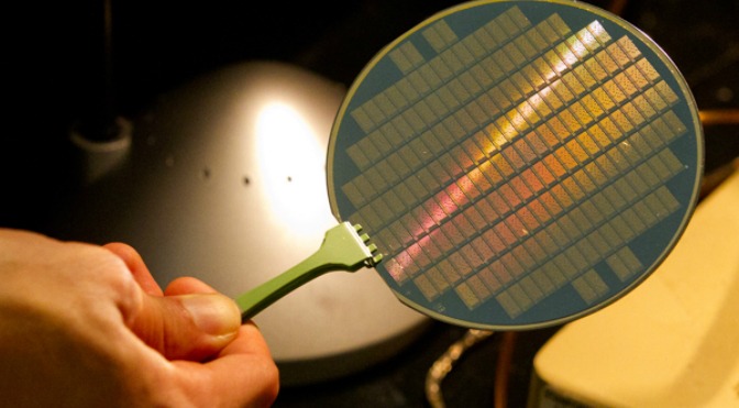
A post silicon computing idea can look strong on paper and still fail if it needs a fantasy factory. This is why commercial-fab work matters. Researchers have shown that carbon nanotube field-effect devices can be made on 200 mm wafers in facilities that already handle silicon production methods, which moves the story away from glass slides and toward manufacturing discipline.
That does not mean mass adoption is near. It means the barrier has changed shape. The hard question is now less “Can this device switch?” and more “Can it switch the same way across a wafer, across months, across many process steps, and under the stress of real products?”
The non-obvious insight is that compatibility may matter more than peak speed. A device that fits existing tools, tolerates lower temperatures, and can sit above silicon may beat a faster material that demands a new factory from scratch. In the U.S., where domestic chip capacity is a policy goal, that practical fit could decide which research leaves the university first.
What Still Blocks Carbon Nanotubes From Replacing Silicon
The main obstacles are not mysterious. They are stubborn. Nanotubes must be placed where designers need them, aligned well enough for circuits, sorted so metallic tubes do not short devices, and connected with low resistance. Each problem has improved. None has disappeared.
Purity and Placement Decide Whether the Promise Survives
A carbon nanotube can act like a semiconductor or a metal depending on its structure. That creates a harsh manufacturing problem. Digital logic wants channels that turn off cleanly. A small number of metallic tubes can create leakage paths and ruin power savings.
Researchers have worked on sorting methods, selective removal, chemical processing, and layout methods that reduce the damage from unwanted tubes. Still, a processor is not a science fair device. It needs millions or billions of transistors behaving within tight limits. That is a far less forgiving test.
Think of it like building a highway from hair-thin lanes. One lane out of place may not matter. Thousands of misplaced lanes create traffic that no driver can predict. The value of CNT transistors depends on controlling the crowd, not admiring one perfect tube under a microscope.
Contacts Can Steal the Win at the Finish Line
Even when the tube itself carries charge well, the metal contact at each end can spoil the result. Contact resistance is the toll booth. If charge struggles to enter or leave the channel, the device loses speed and power benefits before the circuit can use them.
This is where public excitement often gets ahead of the engineering. A material can look ideal in isolation yet struggle at the interface. Real chips are full of interfaces: metal to channel, channel to dielectric, layer to layer, chip to package. The interface is where beautiful theory pays rent.
The counterintuitive lesson is that the weakest part of a future nanotube chip may not be the nanotube. It may be the ordinary-looking connection around it. That is why advanced transistor design basics should matter to business readers too. The winning material is often the one that survives the messy parts of production.
Why 3D Chips May Give Nanotubes Their Best Opening
The cleanest story says nanotubes replace silicon in flat logic chips. The more likely story is messier and more interesting. CNT devices may first shine in vertical designs, where layers of logic and memory sit close together. That path fits the biggest pain in computing today: data movement.
Low-Temperature Processing Changes the Stack
Stacked chips sound simple until you remember heat. If you build one layer, then cook the next layer at high temperature, the first layer may suffer. Nanotube processing can work at lower temperatures than many traditional front-end steps, which makes it attractive for building devices above existing silicon.
That matters for AI hardware because much of the power loss comes from moving data between memory and logic. Put memory and logic closer, and the chip spends less energy acting like a courier. A U.S. foundry-made monolithic 3D prototype that combined conventional silicon, memory, and carbon nanotube devices points toward that direction, even though it remains research hardware.
The surprise is that nanotubes may win by being good neighbors. They do not have to overthrow silicon on day one. They can sit on top, handle selected logic, and help shorten data paths. That is a humbler role, but it may be a smarter one.
AI Workloads Reward Shorter Data Paths
AI systems do a huge amount of repeated math. The math matters, but the movement matters too. Shuffling weights, activations, and intermediate results across a chip burns energy and time. A faster transistor cannot fix all of that if the layout still sends data on long trips.
Energy efficient chips for AI may come from mixing materials with new placement. CNT transistors could support logic in layers where silicon would be harder to add after high-temperature steps. Resistive memory, dense wiring, and vertical logic could work together in designs that look less like old processors and more like compact cities.
For American companies, that could change product strategy. The prize is not only faster cloud training. It is local AI on phones, factory cameras, drones, cars, and medical devices where power budgets are tight. Post silicon computing becomes practical when it solves one painful job better than silicon alone.
Conclusion
The future of computing will not arrive as a clean handoff from one material to another. Silicon has too much factory knowledge, too much design software, and too much economic weight behind it. It will stay in the system for a long time.
The sharper view is that Carbon Nanotube Transistor progress is teaching chip makers where the next openings may appear: low-power logic, vertical stacking, memory-near computing, and devices that can be built with existing production habits. The work is still hard. Purity, contacts, placement, and yield remain serious tests.
Still, the direction is no longer vague. CNT transistors have moved from isolated promise toward circuits, wafers, and foundry-minded process flows. That shift gives U.S. researchers and chip firms a practical target. Do not look for a single silicon-killer headline. Watch for the first narrow product where nanotubes make the system cooler, smaller, or less power-hungry. That is where the new era will begin.
Frequently Asked Questions
How close are carbon nanotube chips to everyday consumer devices?
They are closer than old lab demos, but not close enough to expect mainstream laptops or phones soon. The likelier first use is narrow: stacked chips, sensors, memory-near logic, or research-grade accelerators where power savings justify extra process work.
Why are CNT transistors considered better than silicon for future chips?
They can offer strong gate control at tiny sizes and may switch with lower energy loss. The benefit is not automatic, though. Contacts, tube purity, and manufacturing repeatability decide whether the material advantage survives inside a real circuit.
Will post silicon computing completely replace silicon processors?
A full replacement is unlikely in the near term. A mixed future makes more sense. Silicon can handle many proven layers, while new materials support selected parts where power, heat, or stacking limits hurt current designs.
What is the biggest problem with making nanotube processors?
Manufacturing control is the hardest barrier. Designers need the right tubes in the right places, with consistent behavior across a wafer. A few flawed paths can create leakage, timing errors, or poor yield in large circuits.
Are carbon nanotube devices useful for AI chips?
They could be useful, mainly because AI workloads suffer from heavy data movement and high power use. Nanotube devices may help in vertical chip designs where logic and memory sit closer together, cutting travel distance inside the system.
Why does the United States care about this research?
The U.S. wants stronger domestic chip capacity and more control over advanced computing supply chains. Research that fits existing foundry tools could help American fabs test future devices without rebuilding every part of the manufacturing base.
Do carbon nanotubes make chips faster or more energy efficient?
Both are possible, but energy efficiency may be the more valuable gain. Speed alone does not solve heat and power limits. A chip that performs useful work while wasting less energy can matter more than a small clock-speed win.
What should business leaders watch next in nanotube chip research?
Watch for wafer-scale consistency, foundry-made prototypes, low-temperature 3D stacking, and real circuit demonstrations. Lab records are interesting, but the stronger signal is repeatable hardware made with tools that resemble commercial production.
Related Posts

Palo Alto Networks Cybersecurity Platform Comparison Against CrowdStrike Solutions

Kubernetes Container Orchestration Explained for Non Technical Business Decision Makers